Showing Spotlights 137 - 144 of 332 in category All (newest first):
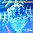
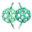 In new work employing the photostrictive effect, researchers have fabricated a flexible two-dimensional (2D) charge transfer molecular (sub-nanometer) nanosheet and observed a sizeable photostrictive effect of 5.7% with fast, sub-millisecond response; this is higher than that of some conventional ferroelectronics and polar semiconductors. This photostrictive effect arises from excess charge carriers induced lattice dilation and conformation change, which is higher than that of some conventional ferroelectronics and polar semiconductors.
Mar 27th, 2018
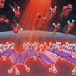
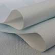 Imagine you are fast asleep in your bedroom when a fire breaks out somewhere else in your house. Fortunately, you have nanotechnology-enhanced wallpaper that detects the fire and automatically rings an alarm. Realizing this idea, scientists have developed a 'smart' wallpaper based on highly flexible fire-resistant inorganic paper embedded with ultralong hydroxyapatite nanowires that serve as the substrate and graphene oxide as the thermosensitive sensor.
Mar 21st, 2018
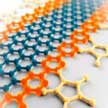
 Single- or few-layer black phosphorus (BP) is one of the most promising two-dimensional semiconductors for electronic and optoelectronic device applications but its environmental instability has always posed a major hurdle for BP-based devices. In contrast, black phosphorus analogues (BPA) nanoarchitectures not only own the similar folded structure of BP, its tunable bandgap energy band and high carrier mobility, but exhibit excellent environmental stability as well. BPA nanosheets can be fabricated by a facile liquid-phase exfoliation method.
Mar 14th, 2018
 Due to its fascinating properties, black phosphorus (BP) has demonstrated appealing potential for not only building (opto)electronic devices, but also in many other areas such as lithium-ion batteries, solar cells, sensors, thermoelectric devices, supercapacitors, and phototherapy. Researchers now have demonstrated that modifying BP with metal ions solved its previous instability problem, which hindered the practical application of BP in electronics and optoelectronics; while at the same time further enhancing the original superior transport properties.
Mar 7th, 2018
 For the first time, liquid-phase exfoliation (LPE) - a widely explored technique to obtain two-dimensional (2D) layered nano-architectures - has been successfully used to exfoliate tellurium, a non-layered material. The resulting 2D Te nanosheets exhibit excellent photoresponse behavior from the UV to the visible regime in association with strong time and cycle stability for on/off switching behavior. This intriguing finding could help in the search for other 2D materials for innovative applications.
Mar 5th, 2018
 Recently, a new member has been introduced to the family of two-dimensional (2D) materials: phosphorene. Phosphorene has attracted much attention because of its tunable direct band gap and superior carrier mobility, but unfortunately phosphorene is subjected to oxidation and degradation under ambient conditions. Now, researchers have reported a facile pathway in obtaining and stabilizing phosphorene through a one-step, ionic liquid-assisted electrochemical exfoliation and synchronous fluorination process. This strategy enabled a novel phosphorene derivative to be discovered - fluorinated phosphorene, which exhibits air-stable photo-thermal properties.
Mar 2nd, 2018
 Scientists report a systematic study involving theoretical and experimental approaches to evaluate the Li-ion storage capability in 2D atomic sheets of nonlayered MoO2. They describe a new process - polymer-assisted reduction - to make atomically flat 2D sheets of MoO2. Since MoO2 is not a 2D material, this process opens a new pathway to make 2D nanostructures from non-layered materials. By successfully making 2D atomic sheets of MoO2, the researchers fabricated a battery electrode in which the Li ion diffusion and electron transport are exceptionally fast.
Feb 15th, 2018
 Researchers have looked closer at the Hall effect in narrow graphene devices - so-called graphene nanoribbons and nanoconstrictions. They were puzzled when they found that the quantization of the conductance was destroyed in some samples - especially because these particular samples were optimized for low edge disorder and low contamination. As it turned out, this effect had been predicted by several theoretical physicists twenty years ago, but largely ignored since no experimental evidence was ever found.
Feb 13th, 2018
 Subscribe to our Nanotechnology Spotlight feed