Showing Spotlights 1361 - 1368 of 2778 in category All (newest first):
 As the semiconductor industry has shrunk the size of transistors they have also had to shrink the size of the masks that define them. Billions of dollars has gone into new technologies to lithographically pattern and define them. Defining these tiny masks has been one of the most difficult parts of making smaller and smaller transistors and a novel nanofabrication approach uniquely side-steps this problem. Researchers at the Kavli Nanoscience Institute have come up with a novel method to three-dimensionally sculpt silicon nanostructures that is easily integrable with existing massively parallel fabrication.
Feb 15th, 2013
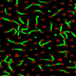
 Carbon nanotubes, like the nervous cells of our brain, are excellent electrical signal conductors and can form intimate mechanical contacts with cellular membranes, thereby establishing a functional link to neuronal structures. There is a growing body of research on using nanomaterials in neural engineering. Carbon nanotube (CNT) synapse circuits are a first step in this direction. In new work, researchers at the University of California, Los Angeles, have developed a CNT synapse with the elementary dynamic logic, learning, and memory functions of a biological synapse.
Feb 12th, 2013
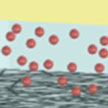
 Quantum dots are expected to deliver lower cost, higher energy efficiency and greater wavelength control for a wide range of products, including lamps, displays and photovoltaics. Unfortunately, the toxicity of the elements used for efficient quantum dot based LEDs is a severe drawback for many applications. Therefore, light-emitting devices which are based on the non-toxic element silicon are extraordinary promising candidates for future QD-lighting applications. Researchers have now demonstrated highly efficient and widely color-tunable silicon light-emitting diodes (SiLEDs). The emission wavelength of the devices can easily be tuned from the deep red (680 nm) down to the orange/yellow (625 nm) spectral region by simply changing the size of the used size-separated silicon nanocrystals.
Feb 8th, 2013
 DNA is a powerful biomaterial for creating rationally designed and functionally enhanced nanostructures. Emerging DNA nanotechnology employs DNA as a programmable building material for self-assembled, nanoscale structures. Researchers have also shown that DNA nanotechnology can be integrated with traditional silicon processing. DNA nanoarchitectures positioned at substrate interfaces can offer unique advantages leading to improved surface properties relevant to biosensing (for instance, graphene and DNA can combine to create a stable and accurate biosensor), nanotechnology, materials science, and cell biology.
Feb 7th, 2013
 The code of conduct for responsible nanosciences and nanotechnologies research (code of conduct) is the Annex to the first nanotechnology-specific legal measure by the EU (2008), a Commission recommendation that is legally nonbinding. The nanotechnologies code of conduct contains principles and guidelines for integrated, safe and responsible (ethical) nanosciences and nanotechnologies research. The central control mechanisms are research prioritisation, technology assessment, ethical and fundamental law clauses/restrictions, defensibility checks and accountability.
Feb 5th, 2013
 Graphene has the potential to revolutionize many fields, especially in electronics to replace the currently used silicon materials. However, graphene does have an Achilles heel: pristine graphene is semi-metallic and lacks the necessary band gap to sever as a transistor. At present, a big challenge for graphene science is how to open a considerable band gap for graphene without significantly degrading its carrier mobility. New theoretical results suggest a rather practical solution for gap opening of graphene and silicene while preserving the desired high carrier mobility, which would allow them to serve as field effect transistors and other nanodevices.
Feb 1st, 2013
 A key benefit of nanoimprint lithography is its sheer simplicity. There is no need for complex optics or high-energy radiation sources with a nanoimprint tool. Especially the nanopatterning of high refractive index optical films promises the development of novel photonic nanodevices such as planar waveguide circuits, nano-lasers, solar cells and antireflective coatings. Researchers have now developed a robust route for high-throughput, high-performance nanophotonics based direct imprint of high refractive index, low visible wavelength absorption materials.
Jan 29th, 2013
 Trace detection of explosives generally involves the collection of vapour or particulate samples and analyzing them using a sensitive sensor system. Various factors, such as wide variety of compounds that can be used as explosives, the vast number of deployment means and the lack of inexpensive sensors providing both high sensitivity and selectivity have made trace detection a very complex and costly task. High sensitivity and selectivity, along with the availability of low-cost sensors, is essential to combat explosives-based terrorism. Nanosensors have the potential to satisfy all the requirements for an effective platform for the trace detection of explosives.
Jan 28th, 2013
 Subscribe to our Nanotechnology Spotlight feed