Research paves the way for next generation of optical tweezers
A team of researchers has created a new method of moving microscopic objects around using micro-robotics.
Feb 14th, 2019
Read moreA team of researchers has created a new method of moving microscopic objects around using micro-robotics.
Feb 14th, 2019
Read more Switching superferromagnetism with electric-field induced strain.
Feb 14th, 2019
Read more Researchers have added a new dimension to their breakthrough technique that expands the capabilities of standard laboratory microscopes.
Feb 14th, 2019
Read more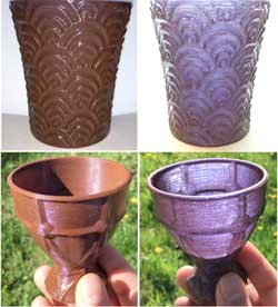 Researchers have 3D printed objects with embedded nanomaterials, showing dichroic effect.
Feb 14th, 2019
Read more Scientists use red phosphorus as spy to keep lithium dendrites in check.
Feb 14th, 2019
Read more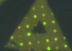 Scientists have developed a way to directly write quantum light sources, which emit a single photon of light at a time, into monolayer semiconductors such as tungsten diselenide.
Feb 14th, 2019
Read more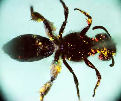 A pollination biologist is using quantum dots to track the fate of individual pollen grains. This is breaking new ground in a field of research that has been hampered by the lack of a universal method to track.
Feb 14th, 2019
Read more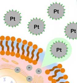 Scientists demonstrated that platinum nanoparticles can be used to kill liver cancer cells with greater selectivity than existing cancer drugs.
Feb 14th, 2019
Read more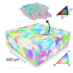 Researchers are working to better understand how shape memory alloys' complex internal microstructures change during shape memory behaviors.
Feb 14th, 2019
Read more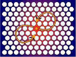 Scientists have discovered a novel type of resonant nanocavity that serves as a 'jail for photons'. The cavity confines light in all three dimensions (3D) simultaneously by exploiting a surrounding photonic band gap crystal nanostructure as the 3D jail's bars.
Feb 14th, 2019
Read more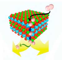 Optimized oxides made from common metals use less energy and show the potential of new design approach.
Feb 14th, 2019
Read more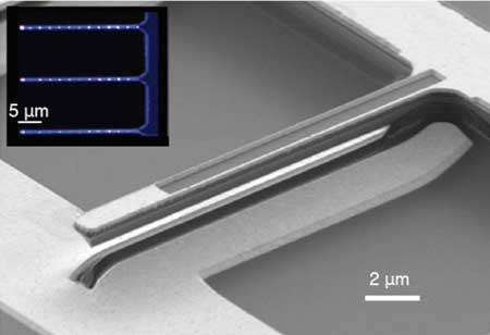 Scientists use implanted silicon ions and electricity to increase the spin time of quantum bits, moving closer to the tech needed for quantum networks.
Feb 14th, 2019
Read more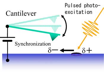 Researchers introduce a new time-resolved microscopy method that allows them to monitor the trajectories of fast-moving charged particles at unprecedented rates.
Feb 14th, 2019
Read more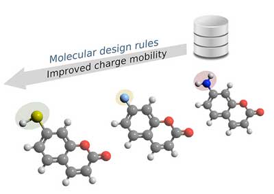 Organic semiconductors often fail to meet expectations regarding efficiency and stability. Researchers are now deploying data mining approaches to identify promising organic compounds for the electronics of the future.
Feb 14th, 2019
Read more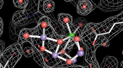 Scientists catch details with atomic resolution, potentially helping design systems to use sunlight and water to produce fuels.
Feb 13th, 2019
Read more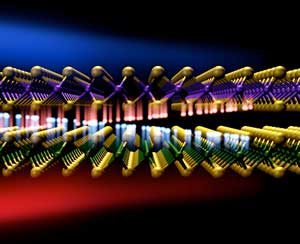 Watching electrons sprint between atomically thin layers of material will shed light on the fundamental workings of semiconductors, solar cells and other key technologies.
Feb 13th, 2019
Read more Subscribe to our Nanotechnology News feed